USB Peripheral
The board includes a Cypress EZ-USB FX2LP.
Cypress’s EZ-USB® FX2LP™ (CY7C68013A/14/15/16A) is a low power, highly integrated USB 2.0 microcontroller. FX2LP has a fully configurable General Programmable Interface (GPIF™) and master/slave endpoint FIFO (8-bit or 16-bit data bus), which provides an easy and glueless connection to popular interfaces such as ATA, UTOPIA, EPP, PCMCIA, DSP, and most processors.
The FX2 can be used in the following ways;
Fully open source firmware for USB JTAG programmer and USB-UART
Fully programmable with open source toolchains.
High speed data transfer reaching real world transfer rates of 30Megabytes/second - 40Megabytes/second.
Emulation support for wide range of USB devices.
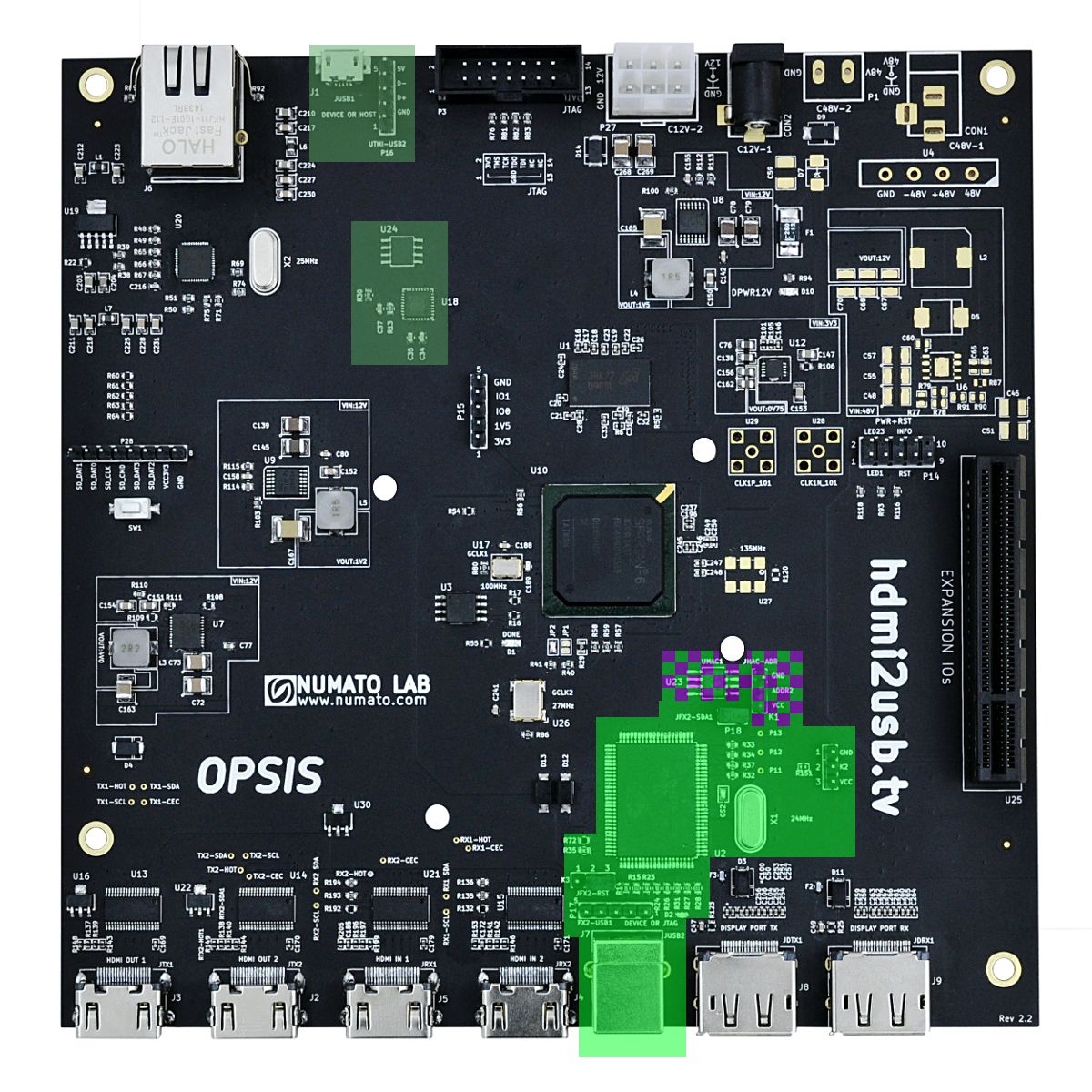
USB Layout
- USB;
- USB OTG (Host or Device) is highlighted in Dark Green
- USB Peripheral (Device Only) is highlighted in Light Green
- Parts shared between Ethernet and USB Peripheral are highlighted in a checkerboard fashion.
Booting
Cypress FX2 Reset Circuit
For the FX2 to boot, the RESET# pin needs to go high.
So the FPGA can reset the FX2, the RESET# pin is connected to the FPGA Pin G22 via jumper JFX2-RST / PXX and a decoupling RC circuit.
The RC decoupling circuit will cause the RESET# pin to go high even if the FPGA is pulling Pin G22 low after XXX ms.
If the FPGA SPI flash is loaded with a gateware which continually toggles Pin G22 low, thus preventing the FX2 from booting properly, the FPGA can be disconnected by removing JFX2-RST / PXX jumper allowing the FX2 to boot.
The preproduction hardware does not have the JFX2-RST / PXX Jumper.
The preproduction hardware "failsafe" circuit on the FX2 reset line
is incorrect.
This means that if the FPGA pulls Pin G22 low the FX2 will never boot!
If the FPGA SPI flash contains no firmware or firmware which has this behaviour
the only way to recover is to use an external JTAG programmer to rewrite the
FPGA SPI flash content.
Location of JFX2-RST / PXX Jumper
XXXXXX
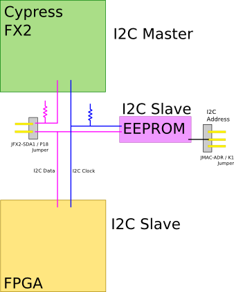
I2C Booting
On boot, the FX2 will try and load it's firmware from an EEPROM connected to the I2C controller.
There are three booting modes possible for the FX2 on the Opsis board;
- If no valid EEPROM is found, the FX2 will boot in "failsafe mode".
- If the real EEPROM is found, the FX2 will boot in "Opsis USB unconfigured mode."
- If a virtual EEPROM is found (provided via the FPGA), the FX2 will boot with a mode selected by the FPGA.
Failsafe Mode - Unable to read EEPROM
This mode is useful when bad information has been written to the EEPROM or the FPGA is preventing correct reading of the EEPROM (and thus the FX2 from connecting to the USB bus).
Enabled this mode by removing the jumper from JFX2-SDA1 / P18. Removing this jumper disconnects the I2C data line of the FX2 from all other devices. As the FX2 will be unable to find an EEPROM to boot from, it will come up in failsafe mode.
The FX2 will connect to USB and appear a "Unconfigured Cypress FX2" with the VID and PID of 04b4:8613. Under Linux it will appear in lsusb as something like this;
# Bus 003 Device 091: ID 04b4:8613 Cypress Semiconductor Corp. CY7C68013 EZ-USB FX2 USB 2.0 Development Kit
After booting in this mode, you can then use the USB firmware loading functionality to reprogram EEPROM / SPI flash.
After booting in failsafe mode, if you wish to program EEPROM you need to put the JFX2-SDA1 / P18 jumper back on without rebooting the FX2. This means it must be done while power is still supplied to the board.
Location of JFX2-SDA1 / P18 Jumper
JFX2-SDA1 / P18 is labelled on the board with both JFX2-SDA1 and P18. JFX2-SDA1 / P18 is a 2 pin header. It can be found just north-east from the Cypress FX2 IC.
See the annotated reference image below;

In the schematic, JFX2-SDA1 / P18 jumper is found in the USB sheet.
Unconfigured Mode - Real EEPROM Booting
The Opsis board has a a Microchip 24AA02E48 2048 kbit EEPROM connected to the FX2.
The EEPROM's primary purpose is to provide a unique MAC address for the Ethernet (which is why it is found in the Ethernet sheet in the schematic) but the user configurable section has been programmed with some extra useful content; * A Cypress FX2 "fallback boot config". * Information about the hardware board revision, manufacture date and batch.
This allows FX2 to be identified as a Numato Opsis board even when the FPGA is unable to provide a full firmware. For the FX2 to find the EEPROM, it needs to be configured with an address of 0b000. This is done by putting the JMAC-ADR / K1 jumper between Pin 2 and Pin 3, pulling the A2 pin low. (The A0 and A1 are permanently pulled low.)
In this mode the FX2 will connect to USB and appear a "Unconfigured Cypress FX2" with the VID and PID of XXXX:XXXX. Under Linux it will appear in lsusb as something like this;
# Bus 003 Device 091: ID XXXX:XXXX Numato Opsis FPGA based open video platform (unconfigured).
Preproduction boards where shipped booting into this mode by default.
Location of MAC EEPROM (UMAC1 / U23)
The MAC EEPROM is labelled on the board with both UMAC1 and U23. The MAC EEPROM is located north-east of the Cypress FX2 IC. The MAC EEPROM is a 8 pin SOIC chip.
See the annotated reference image below;

Location of JMAC-ADR / K1 Jumper
JMAC-ADR / K1 jumper is labelled on the board with both JMAC-ADR and K1. JMAC-ADR / K1 jumper is a 3 pin header. It can be found just north-east from the Cypress FX2 IC.
Pin 1 is the closest to the FX2 IC and labelled VCC. Pin 2 is the middle pin and labelled ADDR2. Pin 3 is the furthest from the FX2 IC and labelled GND.
Connecting the jumper between Pin 1 and Pin 2 causes the A2 pin on the MAC EEPROM to be pulled high.
Connecting the jumper between Pin 2 and Pin 3 causes the A2 pin on the MAC EEPROM to be pulled low.
Never connect Pin 1 and Pin 3 together, this will short VCC to GND and potentially damage the board!
See the annotated reference image below;

In the schematic, JFX2-ADR1 / K1 jumper is found in the Ethernet sheet.
On the preproduction board th JMAC-ADR / K1 Jumper is labelled as JEEADDR.
FPGA "virtual EEPROM" booting
As the FPGA is connected to the FX2's I2C bus, the FPGA can emulate a "virtual EEPROM" and provide the FX2 with firmware.
This allows the firmware provided to the FX2 to be different depending on things like the reset switch state during boot (and thus the type of device the Opsis board appears as).
Connection
The CY7C68013A_100AC is connected to the FPGA in the following way;
Port E is connected to the JTAG programming interface of the FPGA.
- PE0 - TDO
- PE1 - PROG_B
- PE2 - TDI
- PE3 - TMS
- PE4 - TCK
- PE5 - Indicator LED
- PE6 - INIT_B
- PE7 - DONE
- This means FPGALink can be used to program the FPGA using NeroJTAG protocol.
Two hardware UARTs
- Port 0
- RX - Cypress (Pin 41) -> FPGA (Pin P18 / IO_L71N_1) -- Incorrectly labeled CY_RXD1
- TX - FPGA (Pin T17 / IO_L72N_1) -> Cypress (Pin 40) -- Incorrectly labeled CY_TXD1
- Port 1
- RX - Cypress (Pin 43) -> FPGA (Pin P17 / IO_L71P_1) -- Incorrectly labeled CY_RXD0
- TX - FPGA (Pin R17 / IO_L72P_1) -> Cypress (Pin 42) -- Incorrectly labeled CY_TXD0
- Port 0
Port A, Port B, Port C, Port D and RDY+CTL all connected to the FPGA allowing either GPIF Master or Slave FIFO mode operation.
- Full 16 bit external data interface connected for usage in GPIF Master or Slave FIFO mode.
- Almost full GPIF (general programmable interface) connected,
- 8 bit GPIF address out signals
- 6 ready in signals
- 6 control out signals
I2C interface connected to both;
- Small EEPROM for storing VID+PID
- FPGA to allow full 16k ROM to be stored in FPGA's SPI flash
Additional Timer 0 and INT5# connectivity.
Reset controllable via FPGA with fail safe pull up.
Libraries for working with the Cypress FX2
ezusb_io - Easy FPGA interface
fx2lib - Library for programming the FX2 with sdcc
uart - FX2 FPGA firmware which appears as USB UART to computer
jtag - NeroJTAG compatible firmware from FPGALink
More links
